
November
23rd,
2017
- CREATED

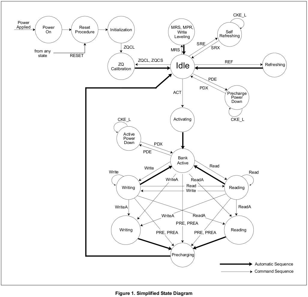
ddr3 device operation timing diagram 요약 분석
Additive Latency(AL)
- Additive Latency (AL) operation is supported to make command and data bus efficient for sustainable bandwidths in DDR3 SDRAM. In this operation, the DDR3 SDRAM allows a read or write command (either with or without auto-precharge) to be issued immediately after the active command. The command is held for the time of the Additive Latency (AL) before it is issued inside the device. The Read Latency (RL) is controlled by the sum of the AL and CAS Latency (CL) register settings.
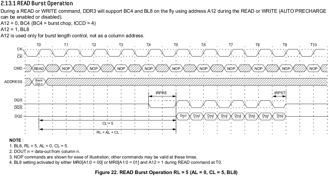
Read Burst Operation
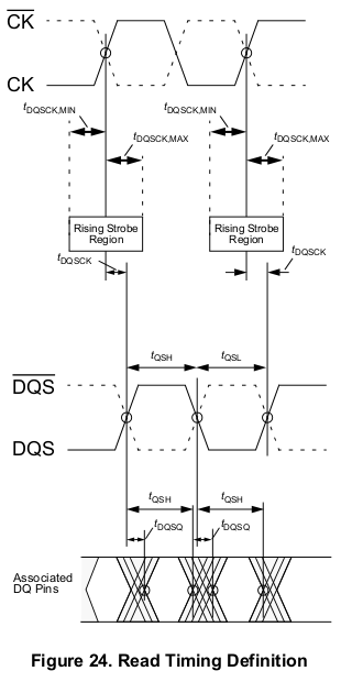
Read Timing Definitions
- Rising data strobe edge parameters: – tDQSCK min/max describes the allowed range for a rising data strobe edge relative to CK, CK. – tDQSCK is the actual position of a rising strobe edge relative to CK, CK. – tQSH describes the DQS, DQS differential output high time. – tDQSQ describes the latest valid transition of the associated DQ pins. – tQH describes the earliest invalid transition of the associated DQ pins.
- Falling data strobe edge parameters: – tQSL describes the DQS, DQS differential output low time. – tDQSQ describes the latest valid transition of the associated DQ pins. – tQH describes the earliest invalid transition of the associated DQ pins. – tDQSQ; both rising/falling edges of DQS, no tAC defined.
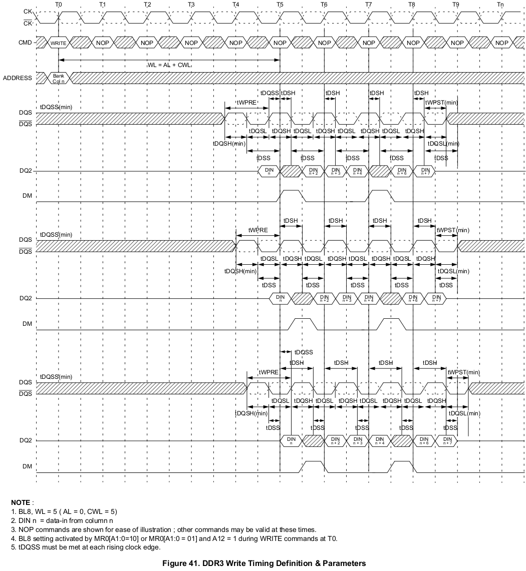
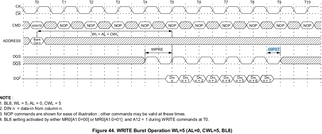
Write Operation
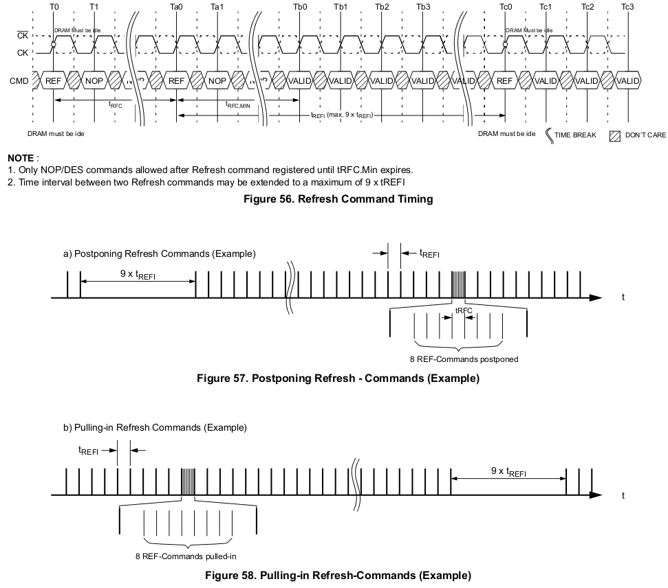
Refresh Command
- REF command는 지속성이 없으므로 매번 실행해야한다. 즉, 새로 고침이 필요하다. tREFI interval 만큼의 시간 간격으로 refresh가 필요하다.
- CS, RAS,CAS가 low 이고 WE 가 rising edge high가 되면 refresh cycle이 시작된다.
- SDRAM의 모든 bank는 최소 tRP 동안 precharged 및 idle 상태여야한다.
- NOP 또는 DES를 제회한 다음 valid command 는 tRFC(min)보다 커야한다. tRFC는 memory density에 따라 다르다.
- delayed 되는 refresh의 총 수는 8개를 초과할 수 없다.
- tRFC : Refresh cycle time
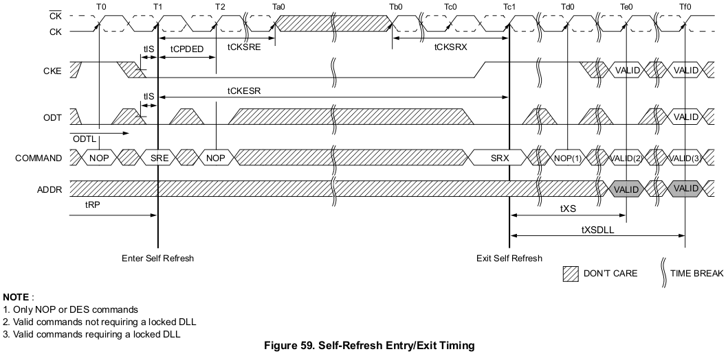
Self-Refresh Operation
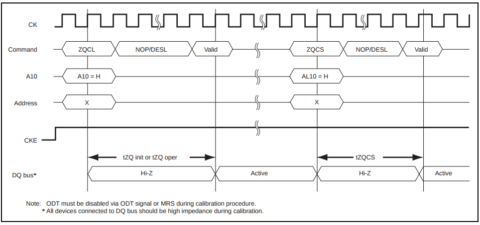
ZQ Calibration
- ZQ calibration command는 PVT 보다 DRAM Ron 및 ODT 값을 보정하는데 사용된다. DDR3 SDRAM은 초기화시 Ron & ODT를 calibration 하는데 오래 시간이 필요하다. – Ron : DQ driver impedance – PVT : process, voltage, temperature
- 어떤 경우에는 ODT 저항 Rtt가 PVT에 따라 변하고, DDR3 SDRAM은 이것을 보정할 수 있다. DDR2에서는 불가능하였다.
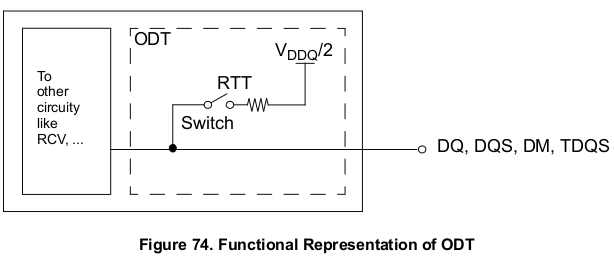
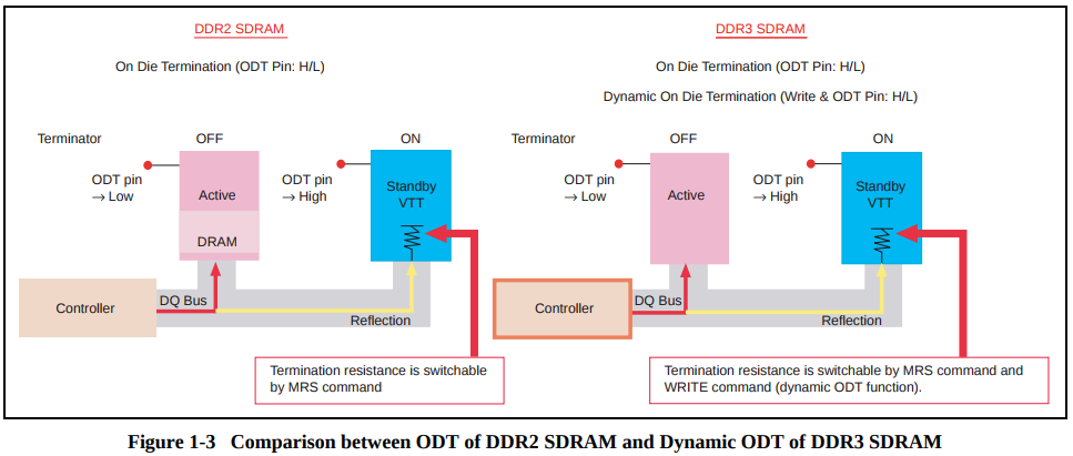
ODT
Write Leveling sequence
- mode register set(MRS) command로 MR1에 write leveling 을 enable 시킨다.
- write leveling mode에서 DDR3 는 DQS rising edge에서 CLK signal을 sampling 하고, DQ pin으로 부터 값을 출력한다.
- controller 에 의해 DQS timing을 shift 시킨다. DQ 출력이 1이 되면 lock 상태로 바뀐다.
MPR : Multi Purpose Register
