November
27th,
2017
- CREATED

Nexell NXP4330 Memory Controller 요약 분석
Overview
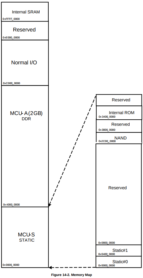
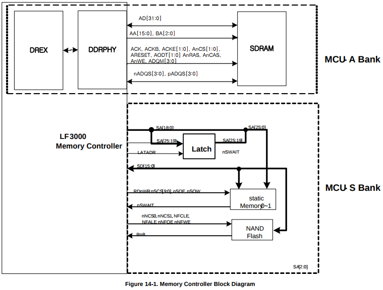
The NXP4330D/Q Memory Controller is based on a Unified Memory Architecture (UMA). This Controller consists of two control units: MCU-A, MCU-S. Each unit has dedicated control pins.
Unified Memory Architecture (UMA)
- Two Separate Memory Controller: – MCU-A : DDR3/LPDDR3/LPDDR2 – MCU-S : Static Memory
- MCU-A features: – MCU-A is organized DREX and DDRPHY – Supports DDR3/LPDDR3/LPDDR2 memory – Supports 8/16/32bit SDRAM of 2GByte – Single Bank of Memory(32bit data bus width) – Supports Power down mode – Supports Self Refresh mode
- MCU-S features: – Static memory – two Static Memory Chip Selects – NAND Flash Interface – 23-bit address supports using latch address – SLC NAND, MLC NAND with ECC(Supports BCH-algorithm) – Static Memory Map Shadow
MCU-A Bank Feature
- Compatible with JEDEC standard LPDDR2-S4/LPDDR3/DDR3 SDRAMs
- Supports 1:2 synchronous operation between bus clock and Memory clock
- Supports up to two memory ranks (chip selects) and 4/8 banks per memory chips
- Supports 512Mb, 1Gb, 2Gb, 4Gb and 8Gbit density per a chip select
- Supports outstanding exclusive accesses
- Supports bank selective precharge policy
- DREX Clock : MBCLK(400MHz)
- MDCLK : MDCLK 0° phase Master DLL clock (400~800MHz). This clock should be the same frequency clock with clk2x in normal mode and generated from the same PLL which MCLK is using. But Master DLL is not able to lock under 400MHz. if MCLK is under 400MHz, the double frequency of clk2x can be used for locking Master DLL for the low frequency operation.