
PHY DS Rev1.22 spec 요약
Overview
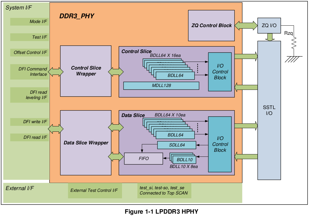
DLL & CONTROL I/F
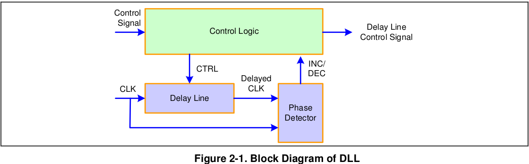
DLL
DLL detects one clock period and generates delay line control signal. Delay line consists of 128 delay cells and is controlled by control logic. Delay line delays input clock and phase detector compares input clock and delayed clock. After phase comparison, phase detector detects whether delayed clock is lag or lead and generates INC/DEC signals to increase or decrease the delay amount of the delay line.
Control
Control block generates address, control and clock signals to I/Os. ADCT[24:0] are reset(RSN)/ODT/address (ADDR)/bank(BA)/chip-select(CS) signals and RAS, CAS, WE are command signals. GATEO and GATEI are DQS clean signals. CK and CKB are differential clock signals. Address and control signals are center aligned at rising CK edge to maximize address/control signal setup/hold timing. GATEO and GATEI signals are used to clean strobe signal, i.e. DQS cleaning. Strobe signal of DDR has high-Z state because it’s bi-directional and this high-z state should be cleaned to be used as a clock signal for memory read transaction.
ZQ Calibration I/O
ZQ_IO calibrates the output and termination impedance and passes through impedance control signals to each I/O cells. (Refer to 8 Application Note). RZQ should be 240ohm.
Signal Description
System Interface Signals
| Name Type | Description |
| clk2x | Input 0° phase system clock. It has strict jitter and duty requirements. Please refer to “UserGuide” for more details. |
| clk_en | Input Clock Enable Signal to synchronize clk2x (PHY clock) with Controller Clock. If the frequency ratio is 1:1, it should be always one. |
| clkm | Input 0° phase Master DLL clock (400~800MHz). This clock should be the same frequency clock with clk2x in normal mode and generated from the same PLL which clk2x is using. But Master DLL is not able to lock under 400MHz. if clk2x is under 400MHz, the higher frequency than clk2x can be used for locking Master DLL for the low frequency operation. (p146) NOTE: All other input signals except for “clkm” should be generated in clk2x domain. The jitter and duty requirement of clkm is the same as that of clk2x. |
| rst_n | Input LOW active reset signal. In normal operation mode, reset is latched by clk2x and latched reset is used for rest of flipflops. This means that clock is required to release the reset of PHY. In scan mode, reset of flipflops are controlled by this pin directly. |
| mode_phy | Input For normal operation, {mode_phy, mode_nand, mode_scan, mode_mux} should be 4’b0000. 0: Normal operation mode. 1: PHY test mode. |
| mode_nand | Input For nand-tree test, {mode_phy, mode_nand, mode_scan, mode_mux} should be 4’b0100. 0: Normal operation mode. 1: Nand-Tree test mode. |
| mode_scan | Input For scan test, {mode_phy, mode_nand, mode_scan, mode_mux} should be 4’b0010. 0: Normal operation mode. 1: Scan test mode. |
| mode_mux | Input For full mux mode, mode_mux should be set. {mode_phy, mode_nand,mode_scan, mode_mux} should be 4’b0001. 1’b0: PHY is used. 1’b1: PHY is not used. |
| mode_highz | Input If this bit is set, output is disabled. |
| mode_run[2:0] | Input Valid only when mode_phy is set. 3’b000: I/O test mode. 3’b001: External PHY read feedback test mode. 3’b010: Internal PHY read feedback test mode. 3’b011: High-Z mode (All outputs are disabled). 3’b100: Internal PHY write feedback test mode. |
| ctrl_hcke | Input This signal decides the reset value of CKE and some signals. If this bit is set, reset value of io_cke_out is 1. Otherwise, reset value of them is 0. |
| ctrl_pd[NS-1:0] | Input This field controls the input buffer of I/O. If this field is set, input buffer is turned-off for power down. This field should be 0 for normal operation. |
| ctrl_wake_up[NS:0] | Input This field controls toggling the input clock of 90 degree phase shift SDLL to save power. “ctrl_wakeup[NS]” for ctrl_slice should be asserted 3 cycles prior to any command and then can be deasserted after the command is given to memory(The controller should issue NOP command during 3 cycles after ctrl_wake_up[NS] is disabled). But if it doesn’t use LPDDR2, “ctrl_wake_up[NS]” can be always deasserted. “ctrl_wakeup[NS-1:0]” for data_slice should be asserted 2 cycles prior to write command and then can be deasserted when ctrl_en falls. For example, if the number of “data_slice” is four, 5’b00000: All input clocks of Slave DLL isn’t toggled. 5’b11111: All input clocks of Slave DLL is toggled.(Default) 5’b10000: The input clock of Slave DLL in ctrl_slice is toggled. But the input clock of SDLL in data_slice isn’t toggled. |
| ctrl_place_type[NS:0] | Input This field decides where each slice should be placed on chip. For example, if data_slice0 is placed on the top or bottom of chip, “ctrl_place_type[0]” should be zero and ioh_* type signals in DS0 should be used to connect with I/O. |
APB Interface Signals
| Name | Type | Description |
| PCLK | Input | APB clock |
| PRESETn | Input | APB reset |
| PADDR[9:0] | Input | APB address |
| PSEL | Input | APB device select |
| PENABLE | Input | APB enable |
| PREADY | Output | APB ready |
| PWRITE | Input | APB direction |
| PWDATA[31:0] | Input | APB write data |
| PRDATA[31:0] | Output | APB read data |
Address & Command Interface Signals
Data Interface Signals
Update, Status And Training Interface Signals
SSTL I/O Interface Signals
Direct Access Interface Signals
Feedback Test Interface Signals
I/O Test Interface Signals
Scan Test Interface Signals
Register Descrition
skip
Functional Description
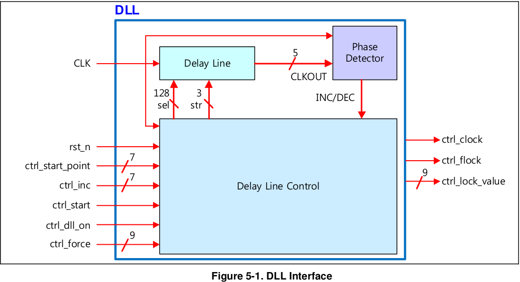 DLL interface signals are shown in Figure 5-1. Delay line consists of 128 delay cells and they are controlled by 128-bit sel signals from delay line control logic. 3-bit str signals are used to control delay line in fine step resolution (fine step delay, tFS) with a quarter of the unit delay of the delay cell.
When ctrl_start becomes HIGH, initial start point and sampling point are loaded with the value of ctrl_start_point(the number of delay cells) and DLL starts running at this initial start point. Initial delay time is calculated by multiplying the unit delay of delay cell and this initial start point. Phase detector starts detecting lead or lag of CLKOUT(delayed multiple phase clock output) in comparison with CLK by sampling CLKOUT at rising edge of CLK. Sampling point is increased or decreased according to this lead or lag information from phase detector.
DLL interface signals are shown in Figure 5-1. Delay line consists of 128 delay cells and they are controlled by 128-bit sel signals from delay line control logic. 3-bit str signals are used to control delay line in fine step resolution (fine step delay, tFS) with a quarter of the unit delay of the delay cell.
When ctrl_start becomes HIGH, initial start point and sampling point are loaded with the value of ctrl_start_point(the number of delay cells) and DLL starts running at this initial start point. Initial delay time is calculated by multiplying the unit delay of delay cell and this initial start point. Phase detector starts detecting lead or lag of CLKOUT(delayed multiple phase clock output) in comparison with CLK by sampling CLKOUT at rising edge of CLK. Sampling point is increased or decreased according to this lead or lag information from phase detector.
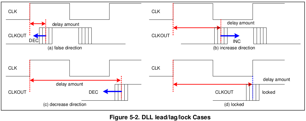 In the case of (a), sampling point is decreased to almost zero
delay, and which is false direction. In this case, initial start point is added with ctrl_inc and this new value becomes
new sampling point.
In the case of (a), sampling point is decreased to almost zero
delay, and which is false direction. In this case, initial start point is added with ctrl_inc and this new value becomes
new sampling point.
Frequency Ratio Clock Definition
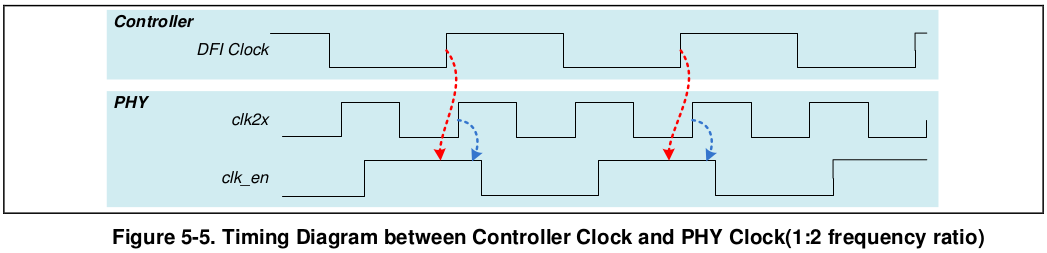 “clk_en” should be always high at both rising edges of “DFI clock” and “clk2x”
DQS clean
Test Mode
skip
Application Note
Initialization
- After power-up and system PLL locking time, system reset(rst_n) is released.
- Select Memory Type (=PHY_CON0[12:11])
– ctrl_ddr_mode=2’b11 (LPDDR3)
– ctrl_ddr_mode=2’b10 (LDDR2)
– ctrl_ddr_mode=2’b00 (DDR2)
– ctrl_ddr_mode=2’b01 (DDR3)
** NOTE: If ctrl_ddr_mode[1]=1’b1, cmd_active=14’h000E(=LP_DDR_CON3[13:0]), cmd_default=14’h000F(=LP_DDR_CON4[13:0]) upd_mode=1’b1(=OFFSETD_CON0[28])
-
Set Read Latency(RL), Burst Length(BL) and Write Latency(WL)
– Set RL in PHY_CON4[4:0].
– Set BL in PHY_CON4[12:8].
– Set WL in PHY_CON4[20:16]. - ZQ Calibration(Please refer to “8.5 ZQ I/O CONTROL PROCEDURE” for more details)
– Enable and Disable “zq_clk_div_en” in ZQ_CON0[18]
– Enable “zq_manual_str” in ZQ_CON0[1]
– Wait until “zq_cal_done”(ZQ_CON1[0]) is enabled.
– Disable “zq_manual_str” in ZQ_CON0[1] - Memory Controller should assert “dfi_init_start” from LOW to HIGH.
- Memory Controller should wait until “dfi_init_complete” is set
– DLL lock will be processed.
Caution: Please don’t change the frequency of “clkm” or voltage during operation. Those conditions should be changed without memory access. After changing, “ctrl_start” should be clear and set to lock again.
- Enable DQS pull down mode
– Set “ctrl_pulld_dqs=9’h1FF” (=LP_CON0[8:0]) in case of using 72bit PHY.
– Please be careful that DQS pull down can be disabled only after Gate Leveling is done. - Memory Controller should assert “dfi_ctrlupd_req” after “dfi_init_complete” is set.
– Please keep “Ctrl-Initiated Update” mode until finishing Leveling and Training. - Start Memory Initialization by memory controller.
- Skip the following steps if Leveling and Training are not required. (Optional features)
– Constraints during Leveling
—— Support BL=4 or 8 during Leveling. (Don’t use BL=16)
—— Not support Memory ODT(On-Die-Termination) during Write DQ Calibration.
– Enable “ctrl_atgate” in PHY_CON0[6].
– Enable “p0_cmd_en” in PHY_CON0[14].
– Enable “InitDeskewEn” in PHY_CON2[6].
– Enable “byte_rdlvl_en” in PHY_CON0[13].
– Recommended that “rdlvl_pass_adj=4” in PHY_CON1[19:16].
– When using DDR3,
—— Set “cmd_active=14’h105E” as default value (=LP_DDR_CON3[13:0])
—— Set “cmd_default=14’h107F” as default value (=LP_DDR_CON4[13:0])
– When using LPDDR2 or LPDDR3,
—— Set “cmd_active=14’h000E” (=LP_DDR_CON3[13:0])
—— Set “cmd_default=14’h000F” (=LP_DDR_CON4[13:0])
– Recommend that “rdlvl_incr_adj=7’h01” for the best margin.
—— Read “ctrl_lock_value[8:0]” in MDLL_CON1[16:8].
—— Update “ctrl_force[8:0]” in MDLL_CON0[15:7] by the value of “ctrl_lock_value[8:0]”.
– Write Leveling (refer to 8.1.1)
– CA Calibration(refer to 8.1.2)
– Gate Leveling (refer to 8.1.3)
—— It should be used only for DDR3 (800MHz).
– Read DQ Calibration(=Read Leveling) (refer to 8.1.4)
– Write Leveling Calibration (refer to 8.1.5)
– After Read DQ Calibration, refer to “T_rddata_en” to know where “dfi_rddata_en_p0/p1” is enabled.
—— Read “T_rddata_en” timing parameters in T_RDDATA_CON0 after Read DQ Calibration.
– Write DQ Calibration (refer to 8.1.6)
– Set “ctrl_dll_on=1” (=MDLL_CON0[5]).
– Set “DLLDeskewEn=1” (=PHY_CON2[12]) to compensate Voltage, Temperature variation during operation.
Caution: Don’t assert “ctrl_ctrlupd_req” during Leveling or Training.I>
- Set “upd_mode=0” (=OFFSETD_CON0[28]) for PHY-Initiated Update.
– If Ctrl-Initiated Update is used, set “upd_mode=1” (refer to 8.7) - Enable and Disable “ctrl_resync”(=OFFSETD_CON0[24])” to make sure All SDLL is updated.
** NOTE: The goal of data eye training (=Read, Write DQ Calibration) is to identify the delay at which the read DQS rising edge aligns with the beginning and end transitions of the associated DQ data eye. By identifying these delays, the system can calculate the midpoint between the delays and accurately center the read DQS within the DQ data eye.
Write Leveling
Write Leveling compensates for the additional flight time skew delay introduced by the package, board and on-chip with respect to strobe(=DQS) and clock.
H/W Write Leveling
S/W Write Leveling
Write Leveling DLL Manual Setting
CA Calibration
Gate Leveling
Write Latency Calibration
Write DQ Calibration(=Write Deskewing)
Low Frequency Operation
ZQ I/O Control Procedure
Termination Resistor Control
